- 您现在的位置:买卖IC网 > Sheet目录323 > DSP56311EVM (Freescale Semiconductor)KIT EVALUATION FOR DSP56311
�� �
�
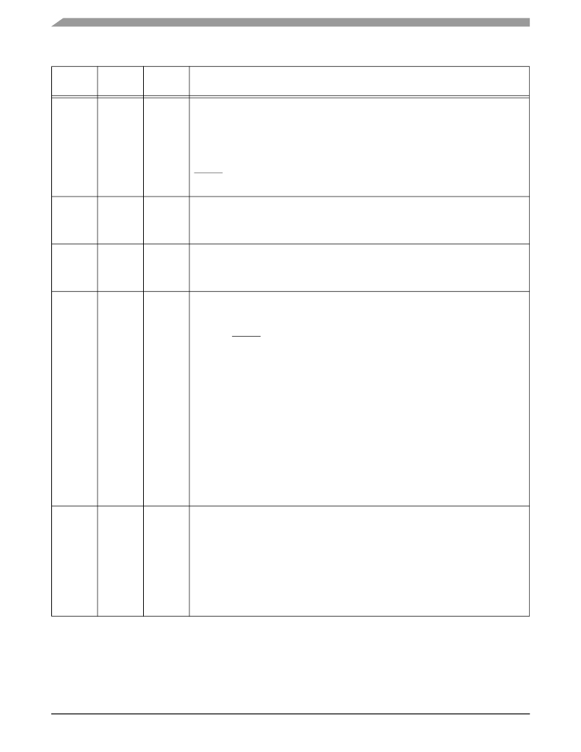
�Serial� Communication� Interface� (SCI)�
�Table� 8-4.� SCI� Status� Register� (SSR)� Bit� Definitions� (Continued)�
�Bit�
�Number�
�4�
�Bit�
�Name�
�OR�
�Reset�
�Value�
�0�
�Overrun� Error� Flag�
�Description�
�Set� when� a� byte� is� ready� to� be� transferred� from� the� receive� shift� register� to� the� receive�
�data� register� (SRX)� that� is� already� full� (RDRF� =� 1).� The� receive� shift� register� data� is� not�
�transferred� to� the� SRX.� The� OR� flag� indicates� that� character(s)� in� the� received� data�
�stream� may� have� been� lost.� The� only� valid� data� is� located� in� the� SRX.� OR� is� cleared�
�when� the� SCI� status� register� is� read,� followed� by� a� read� of� SRX.� The� OR� bit� clears� the�
�FE and� PE� bits;� that� is,� overrun� error� has� higher� priority� than� FE� or� PE.� A� hardware�
�RESET� signal,� a� software� RESET� instruction,� an� SCI� individual� reset,� or� a� STOP�
�instruction� clears� OR.�
�3�
�IDLE�
�0�
�Idle� Line� Flag�
�Set� when� 10� (or� 11)� consecutive� ones� are� received.� IDLE� is� cleared� by� a� start-bit�
�detection.� The� IDLE� status� bit� represents� the� status� of� the� receive� line.� The� transition� of�
�IDLE� from� 0� to� 1� can� cause� an� IDLE� interrupt� (ILIE).�
�2�
�RDRF�
�0�
�Receive� Data� Register� Full�
�Set� when� a� valid� character� is� transferred� to� the� SCI� receive� data� register� from� the� SCI�
�receive� shift� register� (regardless� of� the� error� bits� condition).� RDRF� is� cleared� when� the�
�SCI� receive� data� register� is� read.�
�1�
�TDRE�
�1�
�Transmit� Data� Register� Empty�
�Set� when� the� SCI� transmit� data� register� is� empty.� When� TDRE� is� set,� new� data� can� be�
�written� to� one� of� the� SCI� transmit� data� registers� (STX)� or� the� transmit� data� address�
�register� (STXA).� TDRE� is� cleared� when� the� SCI� transmit� data� register� is� written.� Either� a�
�hardware� RESET� signal,� a� software� RESET� instruction,� an� SCI� individual� reset,� or� a�
�STOP� instruction� sets� TDRE.�
�In� Synchronous� mode,� when� the� internal� SCI� clock� is� in� use,� there� is� a� delay� of� up� to� 5.5�
�serial� clock� cycles� between� the� time� that� STX� is� written� until� TDRE� is� set,� indicating� the�
�data� has� been� transferred� from� the� STX� to� the� transmit� shift� register.� There� is� a� delay� of�
�2� to� 4� serial� clock� cycles� between� writing� STX� and� loading� the� transmit� shift� register;� in�
�addition,� TDRE� is� set� in� the� middle� of� transmitting� the� second� bit.� When� using� an�
�external� serial� transmit� clock,� if� the� clock� stops,� the� SCI� transmitter� stops.� TDRE� is� not�
�set� until� the� middle� of� the� second� bit� transmitted� after� the� external� clock� starts.� Gating�
�the� external� clock� off� after� the� first� bit� has� been� transmitted� delays� TDRE� indefinitely.�
�In� Asynchronous� mode,� the� TDRE� flag� is� not� set� immediately� after� a� word� is� transferred�
�from� the� STX� or� STXA� to� the� transmit� shift� register� nor� when� the� word� first� begins� to� be�
�shifted� out.� TDRE� is� set� 2� cycles� (of� the� 16� � clock)� after� the� start� bit;� that� is,� 2� (16� �
�clock)� cycles� into� the� transmission� time� of� the� first� data� bit.�
�0�
�TRNE�
�1�
�Transmitter� Empty�
�This� flag� bit� is� set� when� both� the� transmit� shift� register� and� transmit� data� register� (STX)�
�are� empty,� indicating� that� there� is� no� data� in� the� transmitter.� When� TRNE� is� set,� data�
�written� to� one� of� the� three� STX� locations� or� to� the� transmit� data� address� register� (STXA)�
�is� transferred� to� the� transmit� shift� register� and� is� the� first� data� transmitted.� TRNE� is�
�cleared� when� a� write� into� STX� or� STXA� clears� TDRE� or� when� an� idle,� preamble,� or�
�break� is� transmitted.� When� set,� TRNE� indicates� that� the� transmitter� is� empty;� therefore,�
�the� data� written� to� STX� or� STXA� is� transmitted� next.� That� is,� there� is� no� word� in� the�
�transmit� shift� register� being� transmitted.� This� procedure� is� useful� when� initiating� the�
�transfer� of� a� message� (that� is,� a� string� of� characters).�
�DSP56311� User’s� Manual,� Rev.� 2�
�8-16�
�Freescale� Semiconductor�
�发布紧急采购,3分钟左右您将得到回复。
相关PDF资料
DSPAUDIOEVMMB1E
BOARD MOTHER DSP563XX
DSPIC30F2010 DEVELOPMENT KIT
KIT DEV EMBEDDED C
DSTRM-KT-0181A
DSTREAM DEBUG AND TRACE UNIT
DSUT1CSU
SURGE SUPPR NETWORK W/GROUND
DTEL2
SURGE SUPPRESSOR PHONE RJ11/RJ45
DV003001
PROGRAMMER PICSTART PLUS 16C/17C
DV164035
MPLAB ICD3 IN-CIRC DEBUGGER
DV164039
KIT DEV PIC24FJ256DA210
相关代理商/技术参数
DSP56311EVMIG_D
制造商:未知厂家 制造商全称:未知厂家 功能描述:DSP56311EVMIG DSP56311EVM Sample Code
DSP56311EVMUM
制造商:未知厂家 制造商全称:未知厂家 功能描述:DSP56311 Evaluation Module Hardware Reference Manual
DSP56311FACT
制造商:未知厂家 制造商全称:未知厂家 功能描述:DSP56311 Higher performance programmable DSP for demanding voice and data applications
DSP56311UM
制造商:未知厂家 制造商全称:未知厂家 功能描述:DSP56311 24-Bit Digital Signal Processor Users Manual
DSP56311UMAD
制造商:未知厂家 制造商全称:未知厂家 功能描述:DSP56311 Users Manual Addendum
DSP56311VF150
功能描述:数字信号处理器和控制器 - DSP, DSC 150Mhz/300MMACS 150Mhz EFCOP RoHS:否 制造商:Microchip Technology 核心:dsPIC 数据总线宽度:16 bit 程序存储器大小:16 KB 数据 RAM 大小:2 KB 最大时钟频率:40 MHz 可编程输入/输出端数量:35 定时器数量:3 设备每秒兆指令数:50 MIPs 工作电源电压:3.3 V 最大工作温度:+ 85 C 封装 / 箱体:TQFP-44 安装风格:SMD/SMT
DSP56311VF150B1
功能描述:数字信号处理器和控制器 - DSP, DSC 24 BIT DSP
RoHS:否 制造商:Microchip Technology 核心:dsPIC 数据总线宽度:16 bit 程序存储器大小:16 KB 数据 RAM 大小:2 KB 最大时钟频率:40 MHz 可编程输入/输出端数量:35 定时器数量:3 设备每秒兆指令数:50 MIPs 工作电源电压:3.3 V 最大工作温度:+ 85 C 封装 / 箱体:TQFP-44 安装风格:SMD/SMT
DSP56311VF150R2
功能描述:数字信号处理器和控制器 - DSP, DSC 24 BIT DSP RoHS:否 制造商:Microchip Technology 核心:dsPIC 数据总线宽度:16 bit 程序存储器大小:16 KB 数据 RAM 大小:2 KB 最大时钟频率:40 MHz 可编程输入/输出端数量:35 定时器数量:3 设备每秒兆指令数:50 MIPs 工作电源电压:3.3 V 最大工作温度:+ 85 C 封装 / 箱体:TQFP-44 安装风格:SMD/SMT